Ko te Tihi Rawa o te Taatari Parakore i roto i nga hau motuhake Hiko mo te Hanga Semiconductor Kore Kore.
Kua whakatapua a Huazhong Gas i a tatou ano ki te mohio ki nga mahi toi me te putaiao o te ahumahi me te hau motuhake hangahanga. I roto i te ao hangarau-nui o enei ra, otira i roto i te hikohiko ahumahi, te hiahia mo parakore ultra-tiketike ehara te hau i te hiahia noa; he tino hiahia. Ka rukuhia e tenei tuhinga te ao arohaehae o tātari poke mo hau motuhake hiko. Ka tirotirohia he aha te mea iti rawa poke Ka whai hua nui, me pehea e kitea ai enei mea uaua tohu poke, me te tikanga mo nga pakihi. Te maramatanga poke hau me nga tikanga mo ratou purenga me te kitenga, penei ICP-MS, Ko te matua ki te whakarite i te pono me te mahi o te ao hou hikohiko. He pai tenei waahanga mo to wa na te mea e tuku ana i te tirohanga a te wheketere-kairoto mo te pupuri i te kaha te ma o nga hau motuhake hiko, he kohatu kokonga o te hikohiko a hikohiko rāngai.
He aha nga hau motuhake hiko me te aha he mea tino nui to ratou ma i roto i te hanga Semiconductor?
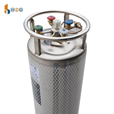
Nga hau motuhake hiko, ka kiia ko hau hiko ranei hau hau, he waahanga ahurei o hau parakore teitei a ranunga hau he mea hanga motuhake mo nga mahi uaua e pa ana ki te hanga i nga waahanga hiko. Whakaarohia ratou ko nga kaihoahoa e kore e kitea o te ao mamati. Ko enei hau e whakamahia ana i roto i te semiconductor Ko te hangahanga he momo rereke, penei i te silane (SiH₄) mo te whakatakoto i nga paparanga silicon, hauota trifluoride (NF₃) mo te horoi ruma, argon (Ar) hei whakangungu rakau, me etahi atu hau doping penei i te phosphine (PH₃) me te arsine (AsH₃) hei whakarereke i nga ahuatanga hiko o hikohiko rauemi. Ko te kupu "motuhake hiko" ko ia ano e whakaatu ana i ta raatau tono whakangao me te tino tika e hiahiatia ana i roto i a raatau hanganga. Ehara enei i a koe i ia ra hau ahumahi; he tino kaha ake o raatau whakaritenga.
Ko te mea nui ki a raatau mā e kore e taea te whakanui ake, ina koa i roto hanga semiconductor. Ko nga iahiko whakauru hou (ICs) e whakaatu ana i nga transistors me nga ara whakahaere he iti rawa, he mea ine i roto i nga nanometers (hau piriona mita). I tenei tauine mokitokito, ahakoa he ngota e kore e hiahiatia—a poke—Ka taea te mahi ano he toka i roto i te awa iti, ka whakararu i te rere hiko e whakaarohia ana, ka pakaru ranei nga hanganga. Ka raru pea te maramara, a, i roto i te umanga e mahia ana nga miriona maramara i runga i te angiangi kotahi, te kino o te putea me te ingoa mai i te whanuitanga. poke ka taea te nui. No reira, te te ma o nga hau motuhake hiko he pou turanga i runga i te katoa hikohiko me te hikohiko tu ahumahi. Tetahi poke ka taea te whakararu i te mahi o te taputapu, te tuku, me te pono, ka kaha hau parakore mana faufaa.
I Huazhong Gas, e mohio ana matou ko o taatau kaihoko kei roto i te ahumahi semiconductor whakawhirinaki mai ki a maatau ki te whakarato hau e tutuki ana, neke atu ranei i "e rima iwa" (99.999%), ara "ono iwa" (99.9999%) nga taumata parakore. Ko te tikanga ko tetahi poke me noho i nga wahanga iti iho i nga wahanga mo ia miriona (ppm) me nga wahanga mo ia piriona (ppb). Te whakatutuki me te manatoko pera purenga teitei me matatau nga taumata purenga tikanga, me te mea nui, matatau tātari poke tikanga. Te aroaro o te ohorere poke Ka taea hoki te tohu i nga take ki te puoto hau te mekameka tuku ranei, he mea nui te arowhai kounga. Ka whakarite maatau Puta hauota Ko nga whakahere, hei tauira, ka tutuki enei paerewa tika, i te mea ko te hauota he hau mahi i roto i te maha o nga waahanga hangahanga hikohiko.
Me pehea e taea ai e nga mea pokekore te whakaheke i nga raina whakangao Semiconductor?
I etahi wa he uaua ki te whakaaro me pehea tetahi mea iti, a tohu poke ka inehia ki nga wahanga mo te piriona (ppb), tae noa ki nga waahanga mo te piriona (ppt), ka raru pea. Engari i te ao o hikohiko hangahanga, enei moroiti poke he hunga kino nui. Kia whai whakaaro tatou ki tetahi tikanga hangahanga hikohiko: he maha, he maha nga waahanga, o nga hikoinga ngawari penei i te tuku (whakatakoto i nga kiriata angiangi), te tarai (tango rauemi), me te whakauru katote (whakauru ngota motuhake). Ko ia taahiraa e whakawhirinaki ana ki tetahi taiao matū e whakahaere tika ana, ka hangaia, ka tiakina ranei e hau motuhake hiko. Mehemea a hau whakamahia i roto i tetahi o enei kaupae kawe i te e hiahiatia poke, tera poke ka taea te whakauru ki roto i nga papanga ngawari o te hikohiko taputapu.
Hei tauira, poke konganuku Pērā i te konutai, te rino, te parahi ranei, ahakoa i te iti rawa o te kukū, ka taea te whakarereke i nga ahuatanga hiko o te silicon. Ka taea e ratou te hanga ara whakahaere kore e hiahiatia, ka ahu atu ki nga ara iahiko poto, ka mahi ranei hei "mahanga" ka aukati i te rere o nga irahiko, ka whakapoipoi i te taputapu, ka ngaro katoa ranei. He poke Ka taea hoki te whakararu i nga tauhohenga matū e whakaarohia ana i roto i tetahi mahi tukanga. Hei tauira, a poke i roto i te hau e werohia ana ka kore e taea te hangai ki raro, ki te nui atu ranei o te wai, ka pakaru nga tauira tika o te angiangi. Ko te paanga ehara i te mea noa ki nga maramara takitahi; he kore kitea poke Ko te take ka paopaohia nga roopu angiangi katoa, ka mutu he miriona taara te ngaronga, te roa o te whakaputanga, me te mahunga o nga apiha hoko penei i a Mark Shen, me whakarite kia mau tonu nga taonga o te kounga. E whakaatu ana tenei i te hiahia nui mo te pakari te inenga poke.
Ko te wero ko te taumata "whakaae" mo tetahi poke kei te mimiti haere tonu hei hikohiko ka iti haere nga ahuatanga o te taputapu. He aha te mea i whakaarohia he pai poke Ko te taumata i te tekau tau ki muri ka raru pea poke i tenei ra. Ko tenei puku kaha mo te whakaheke iti ka nui te pehanga ki nga kaihanga hau me nga taiwhanga tātari kia pai ake rohe kitenga kaha. Ahakoa matūriki nga poke, nga putunga puehu ririki e kore e kitea e te kanohi tahanga, ka taea te aukati i te marama i nga hikoi whakaahua whakaahua, te hanga koha tinana ranei i runga i te mata angiangi. Na reira, te whakahaere i nga kaha katoa poke – ahakoa hau, konganuku, ahakoa matūriki – he mea nui. Ko te awhe poke he maha nga take ka puta, me te whakanui i te hiahia kia matawhānui tātari hau.
He aha nga Rararuraru Nui? Te tautuhi i nga poke i roto i nga hau mo te hikohiko.
Ina korero tatou mo poke i roto i te hau kua whakaritea mo te hikohiko me te hikohiko rängai, kei te titiro mätou ki te huhua o ngä kiripuaki, kei ia tënä he kino nui. Ko enei nga poke kia kitea Ka taea te whakarōpūhia ki te hau, te konganuku, me te matūriki. Ko te mohio ki enei kaitukino noa ko te mahi tuatahi ki te whai hua tātari poke me te whakahaere. Ko te motuhake nga poke kei reira Ka rereke pea i runga i te hau ake, tona tikanga whakaputa, te rokiroki, me te whakahaere.
Karehu poke ko etahi atu hau kei roto i te matua hau motuhake. Hei tauira, in purenga teitei hauota, hau noa poke ko te hāora (O₂), te makuku (H₂O), te hauhā (CO₂), te hauhā (CO), me te hauwai (CHₓ). He tino raruraru te hāora me te makuku i te mea he tino tauhohenga, a tera pea ka arai ki te whakapouritanga o hikohiko rauemi, taputapu tukatuka ranei. Ahakoa i roto i te hau korekore rite argon, ka taea enei i nga taumata tohu. Ka rite ki te kamupene, he maha nga wa ka kite matou i nga tono mo te tātaritanga o a whānui o poke, tae atu ki enei momo tauhohenga. Hei tauira, ko o maatau kaha ko te whakaputa matatini Whakaranu hau hua, kei reira te whakahaere i ia waahanga, tae atu ki te haurehu pea poke, Ko te mea nui.
Ko nga poke konganuku ko tetahi atu raruraru nui. He ngota enei o nga konganuku penei i te konutai (Na), te pāhare pāporo (K), te konupūmā (Ca), te rino (Fe), te parahi (Cu), te nickel (Ni), te chromium (Cr), me te konumohe (Al). Ka puta mai i nga rawa mata, nga taputapu whakaputa (penei i nga paipa me nga reactors), tae noa ki te puoto hau i a ratou ano ki te kore e mahia tikatia. Ka rite ki te korero, enei poke whakarewa ka tino pa ki te mahi hiko o hikohiko nga taputapu. Ki te kimi i enei i nga taumata ppb, ppt ranei, me whai tikanga tātari tino tairongo penei i te Inductively Coupled Plasma Mass Spectrometry (ICP-MS). Me whai whakaaro ano tatou matūriki mea. He matūriki totoka, wai iti ranei e iri ana i roto i te rere hau. Ka taea e ratou te whakararu i te tinana ki nga angiangi, te aukati i nga puha i roto i nga taputapu, te whakauru ranei i etahi atu poke. Ko te tātari he mea matua ki te tango matūriki, engari ko te aro turuki i o raatau taumata he waahanga matawhānui kounga hau hōtaka. Ko etahi hau motuhake hiko he hoki hau pirau ranei hau paitini, e taapiri ana i tetahi atu paparanga uaua ki ta raatau whakahaere me te tātari, me te whakarite kia pai te mahi poke e kore e whakararu ake enei morearea.
ICP-MS: Ko te Paerewa Koura mo te Kite i nga Whakakorenga Kotara i roto i nga hau Semiconductor?
Ina tae mai ki te te tātaritanga o nga poke konganuku i roto hau parakore ultra-tiketike, Inductively Coupled Plasma Mass Spectrometry, or ICP-MS, e kiia ana he hangarau matua. He tikanga wetewete kaha ka taea te kimi me te ine i te whānuitanga o nga momo pokenga huānga, i te nuinga o te wa ka heke iho ki nga taumata iti rawa - whakaarohia nga wahanga-ia-triona (ppt), tae noa ki nga wahanga-ia-taiwha (ppq) mo etahi huānga. Ko tenei tairongo he aha te take ICP-MS kua tino hirahira mo te hikohiko ahumahi, kei hea, pera i ta maatau korero, ara nga tohu iti o poke konganuku ka taea te kino ki kounga hua.
Me pehea ICP-MS mahi ona makutu? I roto i nga kupu ngawari, ko te hau tauira (he otinga ranei i ahu mai i te hau) ka whakauruhia ki roto i te plasma wera rawa, he mea hanga mai argon. Ko tenei plasma, ka eke ki te mahana o te 6,000 ki te 10,000°C, he kaha ki te wawahi i nga ngota ngota hau me te katote i nga ngota kei reira, tae atu ki nga mea katoa. poke konganuku. Ko enei katote ka tangohia mai i te plasma ka arahina ki roto i te irirangi papatipu. Ko te mahi a te spectrometer papatipu he tātari tino tika, ka wehe i nga katote i runga i to raatau tauwehenga papatipu-ki-te utu. A kaitirotiro ka tatau i nga katote mo ia papatipu motuhake, ka taea e tatou te tautuhi ko wai nga huānga kei reira me te aha te rahinga. Te kaha o ICP-MS ki te matawai mo te whanui whanui o poke konganuku i roto i nga hau motuhake i te wa kotahi ka tino whai hua.
Ahakoa ICP-MS he kaha mīharo, ehara i te mea kaore he wero, ina koa ka pa ana hau e whakamahia ana i roto i te semiconductor tito. Ko tetahi huarahi noa ko te mahanga i te poke mai i te nui o te hau ki runga ki te reo kohikohi, ki te wai ranei, ka tātarihia e ICP-MS. Heoi, tika hau werohanga tika ki roto i te ICP-MS Kei te kaha haere tonu te punaha mo etahi tono, ahakoa e hiahiatia ana he atanga motuhake. Ko te whiriwhiri o te tikanga ka whakawhirinaki ki te motuhake poke hau o te moni, te hau matrix, me nga mea e hiahiatia ana rohe kitenga. I Huazhong Gas, he nui ta matou haumi ki nga taputapu tātari hou, tae atu ki ICP-MS kaha, no te mea e mohio ana matou e whakarato pono tātari poke Ko nga raraunga he mea nui ki te whakawhirinaki o taatau kaihoko ki a maatau hiko parakore teitei hau. Te tika o ICP-MS ka awhina ki te whakarite i te te parakore o nga hau ka tutuki nga tono kaha mo kōeke hiko rauemi.
He aha i kore ai e taea te Whakawhitiwhiti te Maama Hau Awekore mo nga Ahumahi Hiko me te Semiconductor?
Ko te hiahia kia kore e aueue hau parakore i roto i te te hikohiko me te ahumahi semiconductor ehara i te mea he manakohanga noa; he whakaritenga taketake e akiakihia ana e te ahupūngao me te ohanga o te hanga taputapu hou. As hikohiko Ko nga ahuatanga o te taputapu ka heke ki te tauine nanometer, to ratou tairongo ki tetahi ahua o poke rangirangi. He poke he iti noa iho i nga mea tawhito, ka taea e nga taputapu nui ake te raru i nga maramara tapahi. Ka pa atu tenei ki nga hua - te paheketanga o nga maramara pai mo ia angiangi - a ahakoa he iti te heke o te hua ka taea te huri ki te miriona taara i roto i nga moni ngaro mo te hikohiko kaihanga.
Whakaarohia te hoahoanga matatini o te miihini miihini hou, te maramara mahara ranei. Kei roto i nga piriona o nga transistors, he mea whakamiharo ia o te miihini iti. Ko te mahi o enei transistors ka whakawhirinaki ki nga ahuatanga hiko o te hikohiko Ko nga rauemi e whakamahia ana, he mea tino whakaraerae poke. Hei tauira, etahi poke konganuku Ka taea e koe te whakauru i nga taumata hiko kore e hiahiatia i roto i te aputa roopu silicon, ka piki ake te rerenga o te waa, ka heke ranei te neke o te kaikawe. Ko te tikanga he puhoi, he iti ake te pai, he taputapu kore mahi ranei. Karehu poke Pērā i te hāora, te makuku rānei ka taea te hanga i nga papa waikura kore, te whakarereke i te matotoru o te kiriata me nga ahuatanga atanga tino nui mo te mahi taputapu. Ko te nuinga kounga hau tika whakamaori ki kounga hua me te pono.
I tua atu, ko te te hikohiko me te ahumahi semiconductor e tohuhia ana e nga tukanga whakangao tino uaua me te utu nui. He kotahi hikohiko Ka taea e te tipu hanga ("fab") te utu piriona taara ki te hanga me te taputapu. Ko te hau whakamahia he mea nui ki te maha o enei mahinga tukanga utu nui. Mehemea a hau motuhake kua poke ki te poke, e kore e pa noa ki nga angiangi e mahia ana i tenei wa; ka taea hoki te whakapoke i nga taputapu tukatuka utu nui ake. Ka roa pea te wa whakaroa mo te horoi me te whakawhiwhi tohu, ka taapiri atu ki nga utu me te whakararuraru i nga raarangi whakangao - he mamae nui mo te tangata penei i a Mark Shen, e whakawhirinaki ana ki te tuku i te waa ki te whakatutuki i nga tono a ana kaihoko. Na reira, te whakarite i te te ma o nga hau motuhake hiko na roto i te uaua tātari poke he rautaki whakaiti morearea mo te katoa o nga mekameka tuku. Ko te arotahi ki runga hau parakore teitei he kahakore na te mea he tino tiketike nga titi.
He aha nga wero matua e pa ana ki a tatou i roto i te tātaritanga o nga poke metara i roto i nga hau motuhake?
Te tātari poke konganuku i roto hau motuhake, otira ko era e whakamahia ana i roto i te hikohiko ahumahi, e whakaatu ana i te huinga ahurei o nga wero. Ko te uauatanga tuatahi i ahu mai i te iti rawa o te kukū o enei poke ka raru pea - he maha nga wa i roto i nga waahanga-ia-piriona (ppb), tae noa ki nga waahanga-ia-triona (ppt). Ko te kimi me te ine tika i enei moni meneti, ehara i te mea ko nga taputapu tātari tino tairongo penei ICP-MS engari he tino maamaa nga taiao-a-alytical me nga tauira kawa whakahaere hei karo i te whakauru o waho. poke.
Ko tetahi wero nui ko te whakauru tauira. He maha hau motuhake whakamahia i roto hikohiko he tino tauhohenga, he pirau, he pyrophoric ranei (ka mura noa i te hau). Ma te haumaru me te whai hua te whakawhiti i enei hau ki te taputapu tātari penei i te ICP-MS me te kore e whakarereketia te hau tauira ki te whakapoke ranei i te taputapu me whai atanga motuhake me nga tikanga whakahaere. Hei tauira, te werohanga tika a hau pirau Pērā i te hauwai pūhaumāota (HCl) ki te paerewa ICP-MS ka tino kino te punaha. Na reira, ko nga tikanga autaki, penei i te mahanga impinger (te mirumiru i te hau ma te wai hei hopu poke) he mahanga cryogenic ranei, he maha tonu nga mahi. Heoi, ka taea e enei tikanga te whakauru i o raatau ake punawai o poke te mate wetewete ranei ki te kore e tino mahia. Ko te whiriwhiri o hau kawe mo te waimehatanga, ki te hiahiatia, me kore e taea mā.
Ko tetahi atu wero ko te "painga matrix." Ko te nuinga hau ake (hei tauira, argon, hauota, hauwai) ka raru te kitenga o tohu poke. Hei tauira, in ICP-MS, te plasma i hangaia mai i te nuinga hau ka taea te hanga katote polyatomic e rite ana te owehenga papatipu-ki-te utu ki etahi o nga whaainga poke konganuku, ka puta ki nga hua pai teka, ki te ine tika ranei. Me whakamahi nga kaitätari i ngä tikanga pënei i te tukinga/tauhohenga i roto i te ICP-MS i te taumira teitei o te matakite papatipu hei whakaea i enei whakapohehetanga. I tua atu, ko nga paerewa whakatikatika e whakamahia ana mo te ine poke whakarewa me tino tika, kia kitea hoki, me whakamana te katoa o nga mahi tātari kia pono ai te pono o te tātari poke hua. Ko matou, hei kaiwhakarato, kei te awangawanga ano mo te pono o puoto hau me to ratou kaha ki te koha poke konganuku i roto i te waa, me haere tonu te whakahaere kounga.
Ka taea e te whakamahi i te taputapu whakawhiti hau te whakapai ake i te tika o te inenga pokekore?
Ae, te whakamahi i te taputapu whakawhiti hau ka taea e koe te whai waahi nui ki te whakarei ake i te tika o te inenga poke, ina koa ka pa ki nga wero hau matrices ranei i te wa e whai ana mo te tino-iti rohe kimi. A taputapu whakawhiti hau, i etahi wa ka kiia ko te punaha whakakore matrix, he mahi ma te tango i te nuinga hau (te waahanga matua o te hau tauira) i te wa e aro ana te tohu poke o te paanga. Ka taea e tenei taahiraa i mua i te aro ki te whakapai ake i te maaramatanga o nga tikanga tātari ka whai ake penei ICP-MS ranei chromatograph hau pūnaha.
Ko te kaupapa kei muri i te tini nga taputapu whakawhiti hau ka whai waahi ki te kiriuhi ahua-permeable, ki tetahi tikanga whakangao/whakahekenga. Hei tauira, ka taea te whakamahi i te kiriuhi palladium hei tango i te hauwai mai i a ranunga hau, tuku i etahi atu poke i roto i te hau kia kukū ka tukuna ki a kaitirotiro. Waihoki, ka taea e nga rauemi adsorbent te mahanga etahi poke mai i te rere hau awa, ka taea te whakakore i te waiariki i roto i te reo iti o te ma hau kawe mo te tātari. Ma te whakaiti i te nui o te nui hau ka tae ki te kaitirotiro, ka whakaitihia e enei taputapu nga pokanoa matrix, ka whakaheke i te haruru papamuri, ka whai hua te whakanui ake i te ōwehenga tohu-ki-haruru mo te whaainga. tohu poke. Ka taea e tenei te heke iho rohe o te kitenga.
Nga painga o te whakamahi i te taputapu whakawhiti hau ka tino kitea i te wa e tātari ana poke i roto i te hiko hau he uaua ki te hapai tika, he nui ranei te pokanoa ki nga taputapu tātari. Hei tauira, i te wa e ngana ana ki te ine i te hikoi, te makuku ranei i roto i te tino tauhohenga hau motuhake, a taputapu whakawhiti hau ka taea pea te wehe i enei poke ki te pai ake hau kawe rite argon helium ranei i mua i to ratou taenga ki te kaitirotiro. Ehara tenei i te whakapai ake i te tika engari ka taea hoki te tiaki i nga waahanga tātari tairongo. Hei kaihanga o 99.999% Purity 50L Cylinder Xenon Gas, e mohio ana matou ki te uara o enei tikanga matatau i roto i te manatoko i te mea motuhake mā o onge me hau motuhake. Ko tenei hangarau ka awhina i nga mea tino nui purenga hau me nga waahanga whakamana.
Te Hononga Tino: Te Tatari Parakore i roto i nga Hau e Whakamahia Totika ki te Hanga Semiconductor.
Ko te hau e whakamahia tika ana i roto i te hanga semiconductor ko te oranga o te tukanga tito. Kei roto i enei ehara i te mea noa hau nui rite hauota me argon, engari ano te whānuitanga o nga momo hau motuhake hiko penei hau epitaxial (hei tauira, silane, germane mo te whakatipu paparanga karaihe), hau werohanga (hei tauira, NF₃, SF₆, Cl₂ mō te tauira), hau implantation katote (hei tauira, arsine, phosphine, boron trifluoride mo te doping), me te haurehu tuku. Mo ia o enei hau e hiahiatia ana, te taumata me te momo e whakaaetia ana poke kua tino tautuhia na te mea ka taea e tetahi rereke te whakamaori tika ki nga hapa o te hikohiko angiangi. Tenei hanga tātari poke mo enei hau tukanga he tino hianga whakahaere kounga.
Whakaarohia te waipara o te paparanga hika hauhā angiangi, he kaitakawaenga noa i roto i nga transistors. Ki te te hāora ka whakamahia te hau mo tenei tukanga he waiwaro poke, ka taea te whakauru i te waro ki roto i te paparanga waikura, ka whakaheke i ona ahuatanga whakamarumaru me te arahi pea ki te kore o te taputapu. Waihoki, ki te he etching hau kei roto he ohorere poke, ka huri pea i te reiti etch, i te whiriwhiringa ranei, ka puta ki nga ahuatanga he nui rawa, he iti rawa, he he ranei te hanga. Ahakoa he poke i roto i te hau korekore rite Puta hau argon ka whakamahia mo te pupuhi ka taea te whakawhiti ki runga i te mata angiangi, ka pa ki te kounga o te kiriata. Te paanga o te poke he maha nga tukanga-motuhake, te tikanga he poke he mea tino nui te whakamanawanui i tetahi taahiraa poke i tetahi atu.
Ko tenei hononga whakahirahira me whai huarahi matawhānui tātari poke. Ehara i te mea mo te tirotiro i te hua whakamutunga; ka whai wāhi ki te aro turuki i ngā rawa mata, ngā kōawa mahi, me te whakamutunga hau nga wahanga purenga. Mo motuhake semiconductor hau, nga whakaritenga mo nga poke i roto i te semiconductor He tino uaua nga tono, e turaki ana i nga rohe o te rapunga tātari. Ka mahi tata matou me o taatau kaihoko i roto i te semiconductor me te hikohiko mara ki te mohio ki o raatau motuhake poke tairongo mō rerekē hau me nga ranunga hau. Ka awhina tenei huarahi mahi tahi ki te whakarite i te hau motuhake parakore he rite tonu ta matou tuku ki te whakatutuki i nga whakaritenga mo o raatau mahi whakangao. Ko te wero kei te kimi a whānui o poke i nga taumata e heke haere tonu ana.
I tua atu i te Taiwhanga: Nga Tikanga Pai mo te Whakahaere i nga hau Semiconductor Puri-Teitei ki te Aukati i te Whakakino.
Te whakarite i te te ma o nga hau motuhake hiko e kore e mutu ina te hau ka wehe i to maatau hangahanga. Te pupuri i tera mā te huarahi katoa ki te waahi whakamahi i roto i a hikohiko Me aro nui a fab ki te whakahaere, te rokiroki, me te tohatoha. Ahakoa te teitei hau parakore ka poke ki te kore e whakahaere tika. I Huazhong Gas, kaore matou e aro noa ki te whakaputa hau parakore teitei engari me tohutohu ano ki o taatau kiritaki nga tikanga pai hei aukati i te awa poke.
Ko nga mahi tino pai ko:
- Tīpakonga Wae: Ko nga waahanga katoa o te punaha tuku hau - tae atu ki puoto hau, nga kaitakawaenga, nga maru, nga ngongo, me nga taputapu - me hanga mai i nga mea e tika ana (hei tauira, he kowiri tira hiko) me te horoi me te whakamana mo parakore ultra-tiketike (UHP) ratonga. Ko te whakamahi i nga rauemi he ka arahi ki waho o te hau poke a poke konganuku rewharewha ki roto i te rere hau.
- Tikanga Pūnaha: Ko te punaha tuku hau me kaha te turuturu. Ahakoa nga paku iti ka taea e te hau poke rite te hāora, te makuku, me te matūriki he mea ki te uru ki te punaha, ka taupatupatu hau parakore. He mea nui te arowhai turuturu i nga wa katoa.
- Nga Tikanga Puring: He mea nui nga tikanga horoi tika i nga wa katoa e hono ana, e huri ana ranei i te rango. Kei roto i tenei ko te horoi i nga raina ki te a hau korekore teitei (penei argon hauota ranei) ki te tango i tetahi hau mau ranei poke. Ko te iti o te horoi he puna noa o poke. He maha nga wa ka tūtohu matou i nga panui horoi aunoa kia rite tonu.
- Taputapu Motuhake: Ma te whakamahi i nga kaiwhakahaere motuhake me nga raina mo te motuhake hau whanau ranei o hau ka taea te aukati i te paheketanga. He mea nui tenei ina huri i waenga i te hau korekore me te reactive ranei hau pirau.
- Te Whakahaere Porotakaro: Puta hau kia tupato te whakahaere kia kore ai e pakaru. Me penapena ki nga waahi kua tohua, kua pai te hau, me te whakahaere pukapuka "tuatahi-mai, tuatahi-waho". Te whakamahi makuku whakatapua me te hāora Ka taea hoki e nga kaitirotiro i nga waahi whakahirahira te awhina ki te aro turuki mo nga whakaurunga o enei mea noa poke.
Mo nga kaihoko penei i a Mark Shen, e hoko hau ana hei hoko atu, hei whakamahi ranei ki nga mahi whakangao, he mea nui te mohio ki enei tikanga whakahaere mo te pupuri kounga hua oati ratou ki o ratou ake kiritaki. He kawenga mahi tahi. Ka whakarite maatau Puta hauwai ko nga hua, hei tauira, ka whakakiia, ka tiakina kia kore ai poke te whakaurunga, engari he rite tonu te mahi a te punaha a te kaiwhakamahi mutunga. Te whawhai ki poke he kaha tonu mai i te whakaputa ki te tono.
Te Tirohanga ki te Poi Karaihe: He aha nga mea hou mo nga ra kei te heke mai ka taea e tatou te tumanako mo te rapunga poke mo nga hau o te karaehe hiko?
Ko te rapu mo te teitei ake mā i roto haurehu kōeke hiko me te tairongo ake te kitenga poke tikanga ko te haere tonu, peia e te tere tamau o te auaha i roto i te hikohiko ahumahi. I te mea ka heke haere nga ahuatanga o te taputapu ki roto i te rohe iti-10 nanometer ka puta mai nga rawa hou me nga hoahoanga (penei i te 3D NAND me te Gate-All-Around transistors), te paanga o te ngoikore tohu poke ka kaha ake te korero. Ma tenei ka whai ahunga whakamua i roto i nga mea e rua purenga hau hangarau me tātari poke kaha.
Ka taea e tatou te tatari kia maha nga ahuatanga:
- Tepe Rapunga Raro: Nga tikanga tātari penei ICP-MS, Gas Chromatography-Mass Spectrometry (GC-MS), me te Cavity Ring-Down Spectroscopy (CRDS) ka tipu tonu, ka pana rohe kimi mo te whanui ake awhe poke heke iho ki nga reanga ppt mati-tahi, ki te rohe ppq ranei. Ma tenei ka hiahia nga mahi hou i roto i nga puna katote, nga kaitirotiro papatipu, me te kaitirotiro hangarau.
- Aroturuki i roto i te waahi me te wa-tūturu: Kei te piki haere te hiahia mo nga punaha tātari ka taea te aro turuki hau parakore i roto i te wa-tūturu, tika i te waahi o te whakamahi i roto i te hikohiko fab. Ma tenei ka taea te kite wawe i tetahi poke nga huihuinga, nga nekehanga ranei poke taumata, kia tere ake te whakatikatika me te whakaiti i te mate hua. Ka whai waahi nui ki konei nga pukoro iti me nga algorithm chemometric matatau.
- Te tātaritanga o nga ranunga hau matatini: Kei te heke mai hikohiko he uaua ake pea nga tukanga ranunga hau me nga wahanga tauhohenga maha. Te tātari poke i roto i enei matrices wero ka hiahia rautaki tātari hou me nga taputapu whakamaori raraunga. Te kaha ki te ine i te poke i roto i tetahi waahanga kaore he pokanoa mai i etahi atu ka tino nui.
- Arotahi ki nga poke "Killer": Ka haere tonu te rangahau ki te tautuhi motuhake nga poke i roto i te semiconductor te tukatuka e pa ana ki te mahi o te taputapu, ki te hua ranei, ahakoa i nga taumata tino iti. Ka kaha ake nga tikanga tātari ki enei "kaipatu" poke.
- Tātari Raraunga me AI: Ko te nui o nga raraunga i hangaia e te hunga matatau tātari poke Ka whakamahia nga punaha ma te whakamahi AI me te ako miihini ki te tautuhi i nga ahuatanga, te matapae pea poke take, me te arotau purenga hau nga tukanga. Ka taea e tenei te awhina i te mana o te kounga kairangi kaua ki te whakaoti rapanga urupare.
I Huazhong Gas, e u ana matou ki te noho ki mua o enei whanaketanga. Ka whakapau kaha matou ki te rangahau me te whakawhanaketanga, me te mahi tahi me nga hoa umanga me nga whare matauranga ki te ahu whakamua i te maatauranga o hau parakore teitei hanga me tātari poke. Mo o taatau kaihoko, tae atu ki te hunga e mohio ana ki te kounga penei i a Mark Shen, ko te tikanga he tuku pono hau motuhake hiko e whakatutuki ana i nga hiahia tipu o te te hikohiko me te ahumahi semiconductor. To tatou whānuitanga o Helium, e mohiotia ana mo tona koretake me te whakamahi i roto i nga tono motuhake, ka whai hua ano mai i enei tirohanga tātari matatau kia iti ai poke taumata.
Nga Taketake Matua hei Maharahara:
- Nga hau motuhake hiko he taketake ki hanga semiconductor, me a ratou mā he kore-whakawhitiwhiti.
- Ahakoa tohu poke, ka inehia ki te ppb, ki te ppt ranei, ka puta he koha nui me te ngaronga o roto hikohiko nga taputapu.
- noa poke i roto i te hau whakaurua etahi atu hau (pēnei i te O₂, H₂O), poke konganuku, a matūriki mea.
- ICP-MS he hangarau kohatu kokonga mo te kimi a whānui o poke, rawa poke konganuku, i nga taumata tino iti.
- Te pupuri hau parakore me tino tika te whakahaere me te pono o te punaha mai i te puoto hau ki te waahi whakamahi hei aukati poke.
- Ka iti ake te heke mai rohe kimi, te aro turuki i te waa tuuturu, me te peia AI tātari poke mo kōeke hiko hau.
- Te whakahaere i nga kaha katoa poke he mea nui mo te whakarite i te kounga hua me te pono o te ao hou hikohiko.